This is default featured slide 1 title

Go to Blogger edit html and find these sentences.Now replace these sentences with your own descriptions.

This is default featured slide 2 title

Go to Blogger edit html and find these sentences.Now replace these sentences with your own descriptions.

This is default featured slide 3 title

Go to Blogger edit html and find these sentences.Now replace these sentences with your own descriptions.

This is default featured slide 4 title

Go to Blogger edit html and find these sentences.Now replace these sentences with your own descriptions.

This is default featured slide 5 title

Go to Blogger edit html and find these sentences.Now replace these sentences with your own descriptions.

Sunday, April 13, 2014

Wireless FM Transmitter Circuit

With MAX2606 we can make a small mono fm transmitter. It is build with MAX2606 and covers at least 20m with 1.5 m long copper wire antenna. You can use this transmitter as an oscillator but change the 1000pF capacitor from the antenna with 15pF.

MAX2606 transmitter output power is -10dBm, that means something around 100µW (micro-watts) = 0.0001W. Of course this is very low, that’s why we recommend you to use an auxiliary power amplifier if you want to build a more powerfull transmitter based on MAX2606. You can find a few fm power amplifiers on electroschematics.com so please use the search box.

Max2606 transmitter circuit diagram

Long Range FM Transmitter

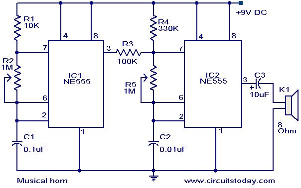
This is very stable, harmonic free, long range fm transmitter circuit which can be used for fm frequencies between 88 and 108 MHz. This can cover 5km range (long distance). It has a very stable oscillator because you use LM7809 stabilizer which is a 9V stabilized power supply for T1 transistor and for frequency adjustment that can be achieved by using the 10K linear potentiometer. The output power of this long range rf transmitter is around 1W but can be higher if you use transistors like KT920A, BLX65, BLY81, 2N3553, 2SC1970, 2SC1971…

T1 is used as an oscillator stage to deliver a low power stable frequency. To adjust the freq. use the 10k linear potentiometer like this: if you trim down, towards ground, the freq. will drop and if you adjust it toward + it will rise. Basically the potentiometer is used as a variable power supply for the two BB139 varicap diodes. Those two diodes act like a variable capacitor when you adjust the pot. By varying the diode capacitance the L1 + diodes circuit makes a resonance circuit for T1. You can use transistors like BF199, BF214 but do not use BCs. At this moment you don’t have yet the long range fm transmitter because the power is quite low, no more than 0.5 mW.

How does long range fm transmitter works

Make sure to encase the oscillator stage in a metallic shield to prevent parasite frequencies destabilizing the oscillating stage.
T2 and T3 works as a buffer stage, T2 as a voltage amplifier and T3 as a current amp. This buffer stage is very important for freq stabilization because is a tampon circuit between the oscillator and the preamp and final amplifier. It is well known that poor transmitter designs tend to modify freq. as you adjust the final stage. With this T2, T3 stage this won’t happen anymore!
T4 is a preamplifier for the fm transmitter and is used as a voltage power rf amplifier and will deliver enough power to the final T5 transistor. As you can see T4 has a capacitor trimmer in its collector, this is used to make a resonance circuit that will force T4 to amplify better and get rid of those unwanted harmonics. L2 and L3 coils must be at 90 degrees angle one to another, this is to avoid frequency and parasite coupling.
The final stage of the long range rf transmitter is equiped with any rf power transistor that has at least 1 watt output power. Use transistors like 2N3866, 2N4427, 2N3553, BLX65, KT920A, 2N3375, BLY81, 2SC1970 or 2SC1971 if you want to have a pro fm transmitter with enough power to cover a long range area. If you use 2N2219 you will get no more than 400mW. Use a good heatsink for the T5 transistor as it gets a little hot. Use a good 12V/1Amp minimum stabilized power supply.
Long range fm transmitter circuit diagram
long range fm transmitter
click on the schematic image for larger view
T1 = T2 = T3 = T4 = BF199
T5 = 2N3866, 2N4427 or 2SC1970 for 1Watt / 2SC1971, BLX65, BLY81, KT920A or 2N3553 for 1.5 to 2W power.
L1 = 5 turns / 0.6mm / 4mm silvered copper
L2 = 6 turns / 0.8mm / 6mm enamelled copper
L3 = 3 turns / 1mm / 7mm silvered copper
L4 = 6 turns / 1mm / 6mm enamelled copper
L5 = 4 turns / 1mm / 7mm silvered copper
Use silvered copper for L3 and L5 if you want to obtain better characteristics.

Adjustments of the long range transmitter

Start by construction the oscillator stage, solder a small wire to T1 10pF capacitor out and listening to a fm receiver, trim the 10k pot untill you can “hear” a blank noise or if you plug in an audio source you can hear the music. With a 70cm wire you can cover a 2 – 3 meter area just with the oscillator stage.
Then continue to build the rest of the rf transmitter, use proper shielding as indicated in the circuit schematic. When you finished the transmitter construction connect the antena or better a 50 or 75 Ω resistive load and use this rf probe, you can use 1N4148 diode instead of the probe diode.
Adjust again the 10k pot to desired freq. and then go to T4 stage and trim the first collector trimmer for maximum voltage indication on the multimeter. Then continue with the next trimmer and so on. Then go back to the first trimmer and readjust again untill you obtain the highest voltage on the multimeter. For 1 watt rf power you can measure a 12 to 16 Voltage. The formula is P (in watt) is equal to U2 / Z, where Z is 150 for 75Ω resistor or 100 for 50Ω resistor, but you must remember that the real rf power is lower.
After those adjustment, if everything is going well connect the antenna, continue using the rf probe, readjust again all the trimmers starting from T3. Make sure you don’t have harmonics, check your TV and radio set to see if there is disturbance on the band. Check this in another room, far away from the fm transmitter or antenna.
That’s all folks :D … This is my design for a long range transmiter and is working well. I used 2SC1971 which has a 12dB power gain in 88 … 108 MHz band, this is around 15 times rf amplification. As T4 delivers around 80 to 100 mW of rf power the final stage has enough power to deliver between 1 to 2W depending the transistor usage.

Good FM Transmitter Circuit

This house FM transmitter for your stereo or any other amplifier provides a good signal strength up to a distance of 500 meters with a power output of about 200 mW. It works off a 9V battery.
The audio-frequency modulation stage is built around transistor BF494 (T1), which is wired as a VHF oscillator and modulates the audio signal present at the base. Using preset VR1, you can adjust the audio signal level.

Audio FM transmitter circuit diagram :
quality fm transmitter circuit schematic
The VHF frequency is decided by coil L1 and variable capacitor VC1. Reduce the value of VR2 to have a greater power output.
The next stage is built around transistor BC548 (T2), which serves as a Class-A power amplifier. This stage is inductively coupled to the audio-frequency modulation stage. The antenna matching network consists of variable capacitor VC2 and capacitor C9. Adjust VC2 for the maximum transmission of power or signal strength at the receiver.
If you design a good pcb layout you can use it as a car fm transmitter.
For frequency stability, use a regulated DC power supply and house the transmitter inside a metallic cabinet. For higher antenna gain, use a telescopic antenna in place of the simple wire. Coils L1 and L2 are to be wound over the same air core such that windings for coil L2 start from the end point for coil L1. Coil winding
details are given below:
L1: 5 turns of 24 SWG wire closely wound over a 5mm dia. air core
L2: 2 turns of 24 SWG wire closely wound over the 5mm dia. air core
L3: 7 turns of 24 SWG wire closely wound over a 4mm dia. air core
L4: 5 turns of 28 SWG wire on an intermediate-frequency transmitter (IFT) ferrite core
Check the related posts for some stereo fm transmitter circuits.

Monday, March 10, 2014

8 function christmas lamp

Description.
This 8 function serial Christmas lamp controller is based on the IC UTC 8156 from Unisonic. Specially designed for the same purpose, the UTC 8156 can control the four lamps in 8 modes namely waves, sequential, slo-gol, chasing/flash, slow fade, twinkle/flash, steady ON and auto scan. Control signals for controlling the lamps will be available at pin 12 to pin 15 of the IC. SCRs are used to drive the lamps according to these control signals.
Circuit diagram.
8 mode christmas lamp
Notes.
  • The circuit can be assembled on a Vero board.
  • L1 to L4 can be 230V/40W lamps.
  • H1 to H4 can be TYN612 SCRs.
  • Heat sinks are recommended for the SCRs.
  • IC1 must be mounted on a holder.
  • If 1A bridge is not available, make one using four 1N4007 diodes.
  • S1 can be an 8 through rotary type selector switch.
  • S1 can be used to select the modes.

Multi-channel audio mixer circuit using LM3900

LM3900 multi-channel audio mixer.

A simple multi-channel audio mixer circuit using LM3900 quad amplifier is given below. The circuit consists of 4 channel quad amplifier (LM3900). Two mic audio inputs and two direct line inputs are available in this circuit. By adding the same circuit parallel with this, you can increase the number of inputs according to the applications. Each input is connected to the inverting terminal of LM3900.The built in amplifier of each section amplifies every audio input separately and is fed to the output terminals. The output terminal from each channel is connected to a single output line with a resistance not greater than 680K and produces a mixed audio at the output with very low noise. This audio mixer circuit doesn’t use a low impedance input to mix ideal sources. Capacitors C1 to C4 are the decoupling capacitors for the corresponding channels. C5 is the output decoupling capacitor.

Circuit Diagram.

lm3900 audio mixer
Multi channel audio mixer circuit

General Description of LM3900.

LM3900 series amplifiers consist of four independent and internally compensated amplifiers that are designed for single and wide power supply voltage. These amplifiers provide a wide range of voltage inputs and very good response for all audio frequencies. They also provide a large output swing.

The architecture and pin configuration of LM3900 is shown in the picture below.

Lm3900 pin configuration
LM3900 pin configuration and architecture

The main features of this audio mixer circuit as compared to the other audio mixers are given below.

1)      Wide range of supply voltage input (4volt to 32volt)
2)      Dual voltage supplies also adoptable (+/- 2.2volt to +/-16volt)
3)      Low input biasing current(30nA)
4)      Providing very high open loop gain(70dB)
5)      Output short circuit protection
6)      Simple and compatible design
7)      Low distortion
8)      Good frequency response

Notes.

  • Assemble the circuit on a good quality PCB.
  • The circuit can be powered from anything between 5 to 30V DC.
  • The power supply must be well regulated and free from any sort of noise.
  • LM3900 must be mounted  on a holder.
  • VR1 to VR4 can be used for adjusting the volume level of the corresponding channels.
  • All fixed resistors are 1/4 watt carbon film type.
  • If the power supply circuit is far from the mixer circuit, then a 100uF/50V electrolytic capacitor must be connected from the positive supply rail to the ground.

Voice modulator circuit

Description.
This is a very versatile voice modulator circuit using IC HT8950A from Holtek Semiconductors. The IC is capable of creating 7 upward or downward steps on the frequency of the input voice at a rate of 8Hz. There is also two special variation effects namely Vibrato mode and Robot mode. This circuit finds a lot of application in systems like telephone, speech processors, toys, mixers etc. A microphone is used to pick up the input voice. Push button switches S2 and S3 can be used for the upward and downward frequency stepping .Push button switch S1 can be used to activate Vibrato mode and push button switch S4 can be used to activate the Robot mode. IC HT82V733 (also from Holtek) is used to amplify the output of the voice modulator.LED D1 indicates the voice level.
Circuit diagram.
voice modulator circuit
Notes.
  • The circuit can be assembled on a Vero board.
  • Do not give more than 4.5v to the circuit.
  • Switches S1 to S4 can be miniature push button switches.
  • S5 can be a miniature ON/OFF switch.
  • K1 can be an 8 ohm speaker.
  • IC1 and IC2 must be mounted on holders

Whistle to beep circuit

Description.
This simple circuit produces a beeping sound that lasts for around 3 seconds whenever you make a whistle. The CMOS Hex inverter CD4049 is the heart of this circuit. Out of the six inverters in CD4049, U1a is wired as an audio amplifier which amplifies the signal picked up by the microphone M1.The U1b is wired as a band pass filter with center frequency around 2KHz.The filter is necessary in order to pass the frequency corresponding to whistling sound and suppress all other frequencies .If the filter is not there, the circuit could easily get false triggered.U1d is wired as a 3S delay monostable multivibrator.The output U1d drives the astable multivibrator formed by U1e and U1f.The astable multivibrator is operating around 4Hz.The combined effect is a intermittent beeping sound that lasts for around 3S.Transistor Q1 is used to drive the buzzer B1.
Circuit diagram with Parts list.
whisle-to-beep-circuit
Notes.
  • Assemble the circuit on a good quality PCB.
  • The circuit can be powered from a 3V battery.
  • IC U1 is a CMOS CD4049 Hex inverter.
  • M1 can be an electret microphone.
  • B1 can be a 3V piezo buzzer.
  • Mount the IC on a holder.
  • The duration of beeping can be adjusted by varying the components C4 and R9.

Ding-Dong sound generator

Description.
This is the circuit diagram of a ding dong sound generator based on two NE555 timer ICs.The circuit is designed to toggle between two adjustable frequencies to produce the ding dong sound. The first NE555 (IC1) is wires as an astable multivibrator operating at 1Hz. The frequency of the second NE555 (IC2) is modulated by the output from the first IC. This is attained by connecting the output of first IC to the control pin (pin5) of the second IC. The tone of the sound depends on the frequency of the second IC and the changeover time depends on the frequency of the first IC.
Circuit diagram.
ding-dong-sound-generator
Notes.
  • The circuit can be assembled on a Vero board.
  • Use 9V PP3 battery for powering the circuit.
  • POT R4 can be used to adjust the tone of the sound.
  • POT R2 can be used to adjust the change over time.
  • IC1 and IC2 must be mounted on holders.
  • K1 can be a 8 ohms, 1/2 watt tweeter

Musical horn circuit.

 Description.
Here is a simple circuit diagram of a simple musical horn using two NE555 ICs. Two ICs are wired as astable mutivibrators. The output of first multivibrator is given to the discharge (pin 7) of the second astable multivibrator. The combined effect of the astable multivibrators produces a musical tone at the output.
 Circuit diagram with Parts list.
musical-horn-circuit.JPG
Notes. 
  • The sound effect can be adjusted by varying the POTs R2&R5.
  • The speaker can be a 8 Ohm tweeter.
  • The circuit can be powered from a 9V PP3 battery.
  • The ICs must be mounted on holders.
  •  All capacitors must be rated 15V.

Micro Flasher

Description.
This micro flasher circuit continuously emits flashing light with the consumption of very less power.The circuit can run for a very long time for four 1.5 V torch cells.

Here a low power CMOS IC CD4093 (IC1) is used to produce sharp pulses  of 20 ms from a red LED.The LED appears to be glowing continuously due to persistence of vision ,and lot of power is saved.The IC1 is quad NAND gate whose one gate is used for producing oscillations.The unused inputs are kept to logic 1 by connecting it to the positive.The value of R1 determines the charging current of C1.

Circuit diagram with Parts list. 
micro-flasher.JPG
Notes. 
  • All capacitors must be rated 10V.
  • The circuit can be easily assembled on a common board.
  • A 6V DC adapter can be also used to power the circuit.
  • The component values need not be strict here. you can find them easily from your junk box.I think you may have to purchase only the IC.

12V Lamp flasher circuit.

Description.
Here is a simple yet powerful circuit that can be used for flashing 12V lamps especially that is used on automobiles.The flashing circuit is based on transistor Q1(BC557) and MOSFET Q2 (IRF530) where the Q2 provides the necessary drive for the lamp.Any number of bulbs can be flashed using this circuit provided that the total load must not exceed 42 Watts.
Circuit diagram with Parts list.
12v-lamp-flasher-circuit.JPG
Notes.
  •  Assemble the  circuit on a good quality PCB or common board.
  • The circuit can be powered form the car battery itself.
  • The switch S1 can be used as the ON/OFF switch.
  • All capacitors must be rated 25V.
  • Slight variations in the flashing frequency is possible by varying the value of C1.

Remote controlled switch circuit

Remote controlled switch for Appliance

Description.

Here is a versatile remote controlled  switch that can ON or OFF any appliance connected to it using a TV remote.
IR remote sensor IC TSOP 1738 is used for receiving the signal. Normally when no signal is falling on IC3 the output of it will be high. This makes Q1 OFF.When a signal of 38 KHz from the TV remote falls on the IC3 its output goes low.This makes Q1 conduct and a negative pulse is obtained at pin 2 of IC 1 NE 555. Due to this IC1 wired as a monostable multivibrator produces a 4 Sec long high signal at its out put.This high out put is the clock for IC 2 which is wired as a Flipflop and of , its two outputs pin 3
goes low and pin 2 goes high. The high output at pin 2 is amplified to drive the relay. For the next signal the outputs of IC2 toggles state.  Result, we get a relay toggling on each press on the remote. Any appliance connected to this circuit can be switched ON or OFF.

Remote Controlled Switch Circuit Diagram with Parts List .

Remote Control Switch Circuit
Remote Controlled Switch Circuit Diagram

Notes:

* Before wiring the circuit make sure that the carrier frequency of the TV remote you have is 38 kHz.For that wire the sensor part only ,point your remote to the TSOP1738 and press any switch.If out put of TSOP1738 goes low then OK, your remote is of 38Khz type.Nothing to worry almost all TV remote are of this type.
* You can use any switch  of the remote because for any switch the code only changes, the carrier frequency remains same.We need this carrier frequency only.
* Assemble the circuit on a good quality PCB or common board.
* The appliance can be connected through NO or NC and C contacts of the relay .
* Use a regulated 6V power supply for the circuit.

Touch Switch Circuit using NE 555

Description

This is the circuit diagram of a small touch plate controller using IC NE 555 .This circuit is ideally useful for making touch operated doorbellsbuzzers,toys etc which when touched on the touch plate operates therelay for a preset time and the turns off automatically.
This circuit is realized by utilizing the high input impedance of trigger pin of the 555 IC.When  the IC is triggered by the induced voltage of human body the output goes high for a time determined by R1 and C1.The transistor is used to drive the relay.The relay contacts can be used to drive the load like bell, motor , lights etc.

Notes.

To make the touch plate cut a 1 square cm thin metal sheet.
To setup the circuit connect to power supply and  adjust R1 while keeping touching on the touch plate.Stop at the point where relay activates.If relay is in the activated state initially then do the same until the relay is deactivated.

Touch Switch Circuit Diagram

touch switch circuit

Flashing LED unit

Description.
The circuit given here is designed as an LED flasher which produces a rotating effect when the LEDs are arranged properly. The circuit has very low current consumption and can be operated from even 3V button cells.
The IC 1 (CMOS NE555) is wired as an astable multivibrator wired at a duty cycle of 50% and 4Hz frequency and drives LEDs D1 to D6.The second IC, IC2 (CMOS NE555) is working as a trigger pulse inverter and drives LEDs D7 to D12.The circuit is arranged such that the ICs sink the current consumed by the LEDs. At low operating voltages like 3V, the CMOS NE 555 performs better when arranged in sinking mode rather than in sourcing mode. The LED D13 remains permanently ON.
Circuit diagram with Parts list.
flashing-led-unit-circuit
LED Arrangement.
flashing-led-unit-led-arrangement

PWM lamp dimmer using NE555

PWM lamp dimmer.

A simple and efficient PWM lamp dimmer using timer IC NE555 is discussed in this article. Yesterdays linear regulator based dimmers can only attain a maximum efficiency  of 50% and are far inferior when compared to the PWM based dimmers which can hit well over 90% efficiency. Since less amount of power is wasted as heat, the switching elements of PWM dimmers require a smaller heat sink and this saves a lot of size and weight. In simple words, the most outstanding features of the PWM based lamp dimmers are high efficiency and low physical size. The circuit diagram of a 12V PWM lamp dimmer is shown below.
We recommend 3 very good books to learn the basics and applications of the 555 timer IC. These books have been thoroughly reviewed and they can be purchased by clicking on this link:- 3 Great Books to Learn 555 Timer Circuits and Projects
12V PWM lamp dimmer
Fig 1 : PWM lamp dimmer using NE555
As you can see, NE555 timer IC which is wired as an astable multivibrator operating at 2.8KHz forms the heart of this circuit. Resistors R1,R2, POT R3 and capacitor C1 are the timing components. Duty cycle of the IC’s output can be adjusted using the POT R3. higher the duty cycle means higher the lamp brightness and lower the duty cycle means lower the lamp brightness. Diode D1 by-passes the lower half of the POT R3 during the charging cycle of the astable multivibrator. This is done in order to keep the output frequency constant irrespective of the duty cycle. Transistors Q1 and Q2 forms a darlington driver stage for the 12V lamp. Resistor R4 limits the base current of transistor Q1.

Understanding the variable duty cycle astable multivibrator.

As I have said earlier, the variable duty cycle astable multi vibrator based on NE555 forms the foundation of this circuit and a good knowledge on it is essential for designing projects like this. For the ease of explanation the timing side of the astable multivibrator is redrawn in the figure below.
astable multivibrator variable duty cycle
Fig 2: Astable multivibrator with variable duty cycle
Upper and lower halves of the POT R3 are denoted as Rx and Ry respectively. Consider the output of the astable multivibrator to be high at the starting instant. Now the capacitor C1 charges through the path R1, Rx, and R2. The lower half of POT R3 ie; Ry is out of the scene because the diode D1 by-passes it. When the voltage across the capacitor reaches 2/3 Vcc, the internal upper comparator flips its output which makes the internal flip flop to toggle its output. As a result the output of the astable multivibrator goes low. In simple words, the output of the astable multivibrator remains high until the charge across C1 becomes equal to 2/3 Vcc and here it is according to the equation Ton =0.67(R1+Rx+R2)C1.
Since the internal flip flop is set now, the capacitor starts discharging through the path R2,Ry into the discharge pin. When the voltage across the capacitor C1 becomes 1/3 Vcc, the lower comparator flips its output and this in turn makes the internal flip flop to toggle its output again. This makes the output of the astable multivibrator high. To be simple, the output of the astable multivibrator remains low until the voltage across the capacitor C1 becomes 1/3 Vcc and it is according to the equation Toff = 0.67(R2+Ry)C1. Have a look at the internal block diagram of NE555 timer shown below for better understanding.
555 timer internal block diagram
Fig3: NE555 internal block diagram
How does the frequency remain constant irrespective of the position of POT3 knob?.
What ever may be the position of  POT3 knob, the total resistance across it remains the same (50K here). If anything decreases in the upper side (Rx) the same amount will be increased in the lower (Ry) and the same thing gets applied to the higher(Ton) and lower(Toff) time periods. The derivation shown below will help you to grasp the matter easily.
With reference to Fig 2, we have:
Ton = 0.67(R1+Rx+R2)C1
Toff= 0.67(R2+Ry)C1
Total time period of the output waveform “T” is according to the equation :
T = Ton + Toff
There fore, T = 0.67(R1+Rx+R2+R2+Ry)C1
                        T= 0.67(R1+2R2+Rx+Ry)C1
We know that Rx+Ry = R3
There fore T = 0.67(R1+2R2+R3)C1
Therefore frequency F = 1/(0.67(R1+2R2+R3)C1) 
From the above equation its is clear that the frequency depends only on the value of the components C1, R1, R2  and the over all value of R3 and it has nothing to do with the position of R3 knob.

Mains Operated LED Circuit

Weekend Projects - Hot/Cold LEDs

Weekend Projects - Little Big Lamp